+91 91524 45255

JTAG Fundamentals

JTAG (Joint Test Action Group) is an interface commonly used for testing, programming, and debugging electronic devices. It allows engineers and developers to access the internal circuitry of a device through a dedicated set of pins known as the JTAG connector.

JTAG Fundamentals

What is JTAG?

JTAG (Joint Test Action Group) is an interface commonly used for testing, programming, and debugging electronic devices. It allows engineers and developers to access the internal circuitry of a device through a dedicated set of pins known as the JTAG connector.

This interface goes beyond basic debugging it can also be used to program onboard flash memory by communicating directly with the flash controller, similar to how ICSP (In-Circuit Serial Programming) works. With JTAG, you're essentially able to peek into the inner workings of a chip, making it a powerful tool in embedded hardware development and reverse engineering.

JTAG diagram

The Need for JTAG

JTAG was developed in the late 1980s to address the growing challenges manufacturers faced when testing assembled PCBs packed with increasingly dense components. Traditional testing methods like bed-of-nails or in-circuit testing were becoming less effective and more complicated due to limited physical access.

To overcome this, a group of manufacturers collaborated on a standardized solution: embedding dedicated test logic directly into the chips themselves. This approach allowed for internal testing and debugging via a standardized interface, paving the way for what we now know as the JTAG protocol.

Boundary Scan

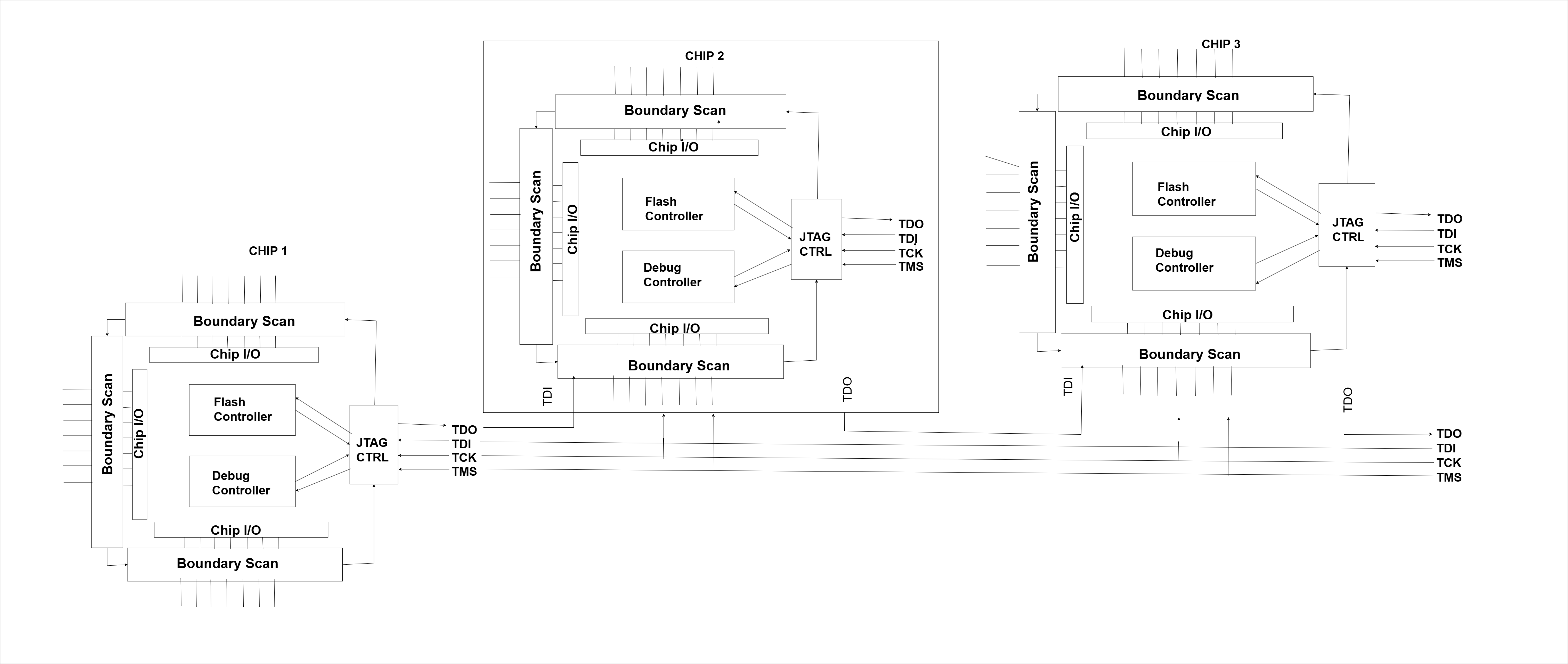
JTAG is often referred to as Boundary Scan Testing because one of its primary uses is testing connections on a chip or PCB without needing direct physical access to internal circuitry.

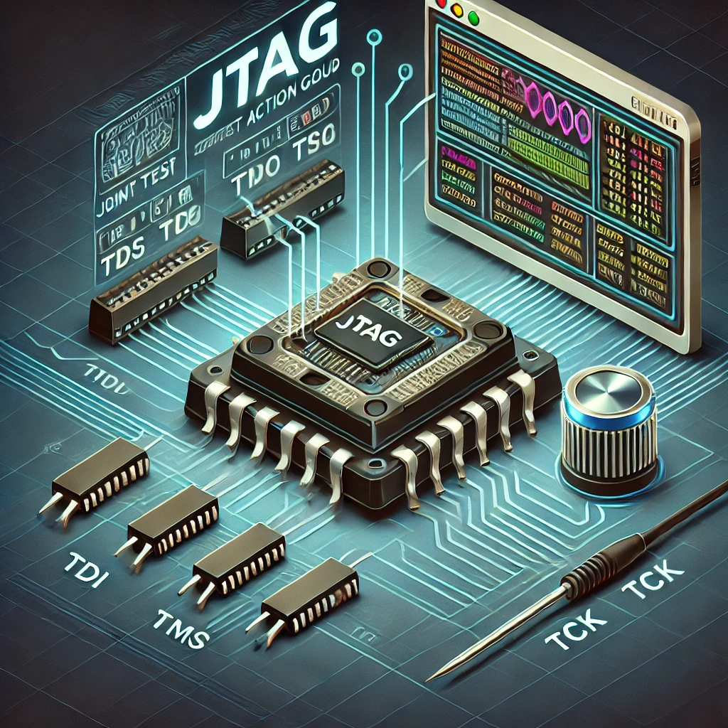
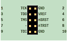
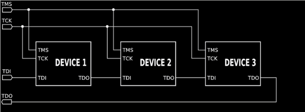
JTAG operates through a serial communication interface that uses a specific set of pins:

JTAG Pin Functions

  • TDI (Test Data In): Sends data into the device.
  • TDO (Test Data Out): Outputs data from the device.
  • TMS (Test Mode Select): Controls the state transitions of the JTAG state machine.
  • TCK (Test Clock): Provides the clock signal for synchronizing data transfer.
  • TRST (Test Reset): An optional pin used to reset the test logic.
JTAG boundary scan diagram

The boundary scan cells are small logic elements inserted between a chip's core logic and its input/output (I/O) pins. Think of them as checkpoints placed right at the edge (or boundary) of the chip. These cells form a scan chain a single line of serial data that flows through each cell and out to the other end.

When the chip powers on, boundary scan logic stays passive and allows signals to pass normally between the core and the I/O. But when JTAG is activated, it can take control of these cells, shifting test data in and out using the scan chain.

Board Testing

Test board level interconnects and diagnose faulty solder joints or broken traces.

Signal Validation

Validate signal paths without needing probes or oscilloscopes.

In short, boundary scan turns your chip into its own testing tool very handy when you're dealing with dense PCBs or tightly packed BGA components.

Daisy Chain

In a daisy chain configuration, multiple JTAG-enabled components are connected in a linear sequence. The output of one device becomes the input of the next, forming a chain-like structure. This setup allows a single JTAG interface to access and control multiple devices in order.

Daisy Chain Configuration

  • The TDO (Test Data Out) of the first chip is connected to the TDI (Test Data In) of the second chip, and so on.
  • This continues until all devices are linked in the chain.
JTAG daisy chain diagram

While this method is efficient and reduces the number of individual connections needed, it does come with a limitation. If you want to extract data from a specific chip say, the first one in the chain you still need to shift through all the devices ahead of it. This process depends on the position of the device in the daisy chain.

Understanding how the chain is arranged helps in identifying which device is being accessed and ensures proper communication during testing, programming, or debugging.

Advantages of JTAG

Direct Access

Provides straightforward access to internal components through a simple pin interface.

No Boot Required

Access system even when device won't boot, useful for debugging bricked devices.

Multi-Device Support

Control multiple devices through a single interface using daisy chaining.

Standardized Interface

Uniform and reliable interface supported by many modern devices.

Limitations of JTAG

Production Locks

Often disabled or locked in production devices to prevent unauthorized access.

Device-Specific

Implementation varies significantly between different manufacturers and chips.

Pin Identification

Requires accurate identification of TDI, TDO, TCK, and TMS pins, which can be undocumented.

Slow Transfer

Serial interface not ideal for transferring large amounts of data quickly.

Looking Ahead!!

JTAG provides low-level access for testing, debugging, and programming devices even when they won't boot. We've covered its fundamentals, boundary scan, and daisy chaining but the real challenge begins with finding the actual JTAG pins on a device.

In the next blog, we'll explore how to identify JTAG pinouts and begin establishing a connection one pin at a time.

Ready to Master JTAG Testing?

Contact us for advanced hardware security assessments and JTAG testing services.

GET ASSESSMENT